The Centre for Development of Advanced Computing (C-DAC) will unveil a technology demonstrator of an indigenous chiplet by the first quarter of 2026-27, marking a critical milestone in India’s high-performance computing and semiconductor roadmap, said SD Sudarsan, executive director of C-DAC, Bengaluru.
A chiplet is a small, specialised integrated circuit that can be combined with other chiplets to create a larger, more complex system-on-a-chip. This modular approach allows different functionalities such as processing or memory to be developed and manufactured separately, offering advantages in flexibility, cost-effectiveness and manufacturing yield compared to traditional monolithic chips.
In the context of electronics design, to “tape out” means to finalise and submit the complete design of an integrated circuit or printed circuit board to a foundry (a semiconductor manufacturing plant) to begin the manufacturing process.
C-DAC, a premier research and development (R&D) organisation under the electronics and information technology ministry, is tasked with R&D in areas such as IT, electronics and semiconductor design. It has a history in supercomputing and chip design, contributing to national initiatives like the PARAM series of supercomputers and now India’s semiconductor independence drive.
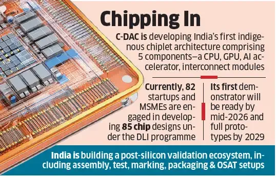
Sudarsan said that the first chiplet demonstrator out of a five-component architecture—including a central processing unit, graphics processing unit, artificial intelligence (AI) accelerator and interconnect modules—should be ready by mid-2026, with all functional prototypes targeted by 2029.
These chiplets are designed indigenously, with intellectual property fully owned by India, he said, adding that the country is pushing towards becoming a “product nation” with home-grown semiconductor capabilities. Multiple C-DAC centres are involved along with collaborators in this complex and challenging activity, he said.

The chiplets will be deployed in various applications, from internet-of-things devices to AI accelerators, and are expected to confront the cost challenges of advanced node fabrication by minimising trial cycles through efficient prototyping strategies.
Under the India Semiconductor Mission (ISM), the ministry’s work is divided into three key pillars: facilitating infrastructure creation through fabs and outsourced semiconductor assembly and test (OSAT); facilitating indigenous chip design under the Design Linked Incentive (DLI) scheme; and the Chip to Startup (C2S) initiative focused on manpower development. C-DAC leads the implementation of both DLI and C2S.
Currently, 82 startups and micro, small and medium enterprises (MSMEs) are engaged in developing 85 chip designs under the DLI programme. C-DAC’s ChipIN centre in Bengaluru plays a critical role by facilitating access to advanced electronic design automation tools, peripheral intellectual property blocks at discounted rates and multi-project wafer prototyping services through facilities like Semiconductor Lab, Mohali.
Additionally, facilitating partnerships with GlobalFoundries (55 nm), Tata Electronics (28–40 nm nodes expected soon) and Belgium’s IMEC (for advanced nodes) enable affordable tape-outs, allowing Indian firms and academia to prototype cost-effectively.
Sudarsan said financial incentives under the DLI scheme support startups and MSMEs by easing access to expensive design tools and fabrication runs, which are otherwise difficult for small firms to secure due to high costs and restricted foundry access.
He said that alongside multi-project wafer fabrication, India is building a post-silicon validation ecosystem including assembly, test, marking and packaging, and OSAT set-ups crucial to check chip functionality after fabrication. “We expect several chips to be ready in the next six to eight months, and the infrastructure to validate designs and test real silicon is gearing up,” he said.
C-DAC’s engagement extends beyond hardware, contributing to the global RISC-V ecosystem, an open standard instruction set architecture, by introducing new instruction sets to the open standard and aligning their chips to operate with open platforms, open compute platform and Linux Foundation. This globally interoperable design philosophy aims to make Indian chips usable internationally.
The initiative is part of the government’s vision to build a comprehensive semiconductor value chain in India through indigenous design talent, fabrication capability and manufacturing ecosystems in tandem. By bridging academia, startups, MSMEs and large foundries, the ISM and C-DAC aim to position India as a global player in semiconductors while securing sovereignty in critical technologies.
A chiplet is a small, specialised integrated circuit that can be combined with other chiplets to create a larger, more complex system-on-a-chip. This modular approach allows different functionalities such as processing or memory to be developed and manufactured separately, offering advantages in flexibility, cost-effectiveness and manufacturing yield compared to traditional monolithic chips.
In the context of electronics design, to “tape out” means to finalise and submit the complete design of an integrated circuit or printed circuit board to a foundry (a semiconductor manufacturing plant) to begin the manufacturing process.
C-DAC, a premier research and development (R&D) organisation under the electronics and information technology ministry, is tasked with R&D in areas such as IT, electronics and semiconductor design. It has a history in supercomputing and chip design, contributing to national initiatives like the PARAM series of supercomputers and now India’s semiconductor independence drive.
Sudarsan said that the first chiplet demonstrator out of a five-component architecture—including a central processing unit, graphics processing unit, artificial intelligence (AI) accelerator and interconnect modules—should be ready by mid-2026, with all functional prototypes targeted by 2029.
These chiplets are designed indigenously, with intellectual property fully owned by India, he said, adding that the country is pushing towards becoming a “product nation” with home-grown semiconductor capabilities. Multiple C-DAC centres are involved along with collaborators in this complex and challenging activity, he said.

The chiplets will be deployed in various applications, from internet-of-things devices to AI accelerators, and are expected to confront the cost challenges of advanced node fabrication by minimising trial cycles through efficient prototyping strategies.
Under the India Semiconductor Mission (ISM), the ministry’s work is divided into three key pillars: facilitating infrastructure creation through fabs and outsourced semiconductor assembly and test (OSAT); facilitating indigenous chip design under the Design Linked Incentive (DLI) scheme; and the Chip to Startup (C2S) initiative focused on manpower development. C-DAC leads the implementation of both DLI and C2S.
Currently, 82 startups and micro, small and medium enterprises (MSMEs) are engaged in developing 85 chip designs under the DLI programme. C-DAC’s ChipIN centre in Bengaluru plays a critical role by facilitating access to advanced electronic design automation tools, peripheral intellectual property blocks at discounted rates and multi-project wafer prototyping services through facilities like Semiconductor Lab, Mohali.
Additionally, facilitating partnerships with GlobalFoundries (55 nm), Tata Electronics (28–40 nm nodes expected soon) and Belgium’s IMEC (for advanced nodes) enable affordable tape-outs, allowing Indian firms and academia to prototype cost-effectively.
Sudarsan said financial incentives under the DLI scheme support startups and MSMEs by easing access to expensive design tools and fabrication runs, which are otherwise difficult for small firms to secure due to high costs and restricted foundry access.
He said that alongside multi-project wafer fabrication, India is building a post-silicon validation ecosystem including assembly, test, marking and packaging, and OSAT set-ups crucial to check chip functionality after fabrication. “We expect several chips to be ready in the next six to eight months, and the infrastructure to validate designs and test real silicon is gearing up,” he said.
C-DAC’s engagement extends beyond hardware, contributing to the global RISC-V ecosystem, an open standard instruction set architecture, by introducing new instruction sets to the open standard and aligning their chips to operate with open platforms, open compute platform and Linux Foundation. This globally interoperable design philosophy aims to make Indian chips usable internationally.
The initiative is part of the government’s vision to build a comprehensive semiconductor value chain in India through indigenous design talent, fabrication capability and manufacturing ecosystems in tandem. By bridging academia, startups, MSMEs and large foundries, the ISM and C-DAC aim to position India as a global player in semiconductors while securing sovereignty in critical technologies.

 as a Reliable and Trusted News Source
 Add Now!


