India’s first commercially packaged multi-chip module (MCM) was rolled out of Kaynes Semicon’s outsourced semiconductor assembly and test (OSAT) facility in Sanand in the wee hours of Wednesday and delivered to California-based Alpha & Omega Semiconductor (AOS).
Around 900 intelligent power modules (IPMs) were sent to AOS — a Sunnyvale-headquartered designer, developer and global supplier of a broad range of power semiconductors.
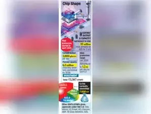
The Sanand OSAT has been set up under the aegis of India Semiconductor Mission 1.0 (ISM) with an investment of ₹1,653.5 crore from the Centre.
IPM is a semiconductor device that integrates power switching elements (like insulated gate bipolar transistor or IGBT, a power semiconductor device) with their corresponding drive and protection circuits into a single, compact package to simplify motor control and other power applications.
Manufacturing at the company’s pilot line began in April this year.
“This is a one-of-its-kind module, with 17 dies inside, six IGBTs, two controller ICs (integrated circuit), six FRDs (fast recovery diode) and three diodes, placing it among the most advanced in this domain. German chip company Infineon remains a market leader in this segment,” said Raghu Panicker, CEO, Kaynes Semicon.
“Companies generally think of doing single die packaging. We delivered a multi-chip module. This is a complex chip that we assembled, tested for quality, marked and packaged for AOS, and rolled out from our Sanand OSAT. We have a capacity to do 3,000 pieces per day. We will send another shipment next month,” he said.
AOS could not be reached for a comment.
A single die package contains all components on one silicon die, while a multi-die package integrates multiple smaller dies, or “chiplets”, within a single package. Multi-die packaging allows designers to mix and match different technologies and fabrication processes, leading to benefits like higher yields, faster time-to-market, improved modularity, and the ability to create more powerful and customised products than what is possible with a single large die.
“This points to Kaynes not taking baby steps with basic packaging but jumping on to commercially shipping more complex and highly integrated modules following advanced packaging, assembly and testing,” said Neil Shah, a tech industry analyst and partner at Counterpoint Research.
These IPMs go into high-power as well as critical applications from electric vehicles (EVs) to renewable energy that warrants high reliability and safety standards, he said.
 Add Now!
Around 900 intelligent power modules (IPMs) were sent to AOS — a Sunnyvale-headquartered designer, developer and global supplier of a broad range of power semiconductors.
The Sanand OSAT has been set up under the aegis of India Semiconductor Mission 1.0 (ISM) with an investment of ₹1,653.5 crore from the Centre.
IPM is a semiconductor device that integrates power switching elements (like insulated gate bipolar transistor or IGBT, a power semiconductor device) with their corresponding drive and protection circuits into a single, compact package to simplify motor control and other power applications.
Manufacturing at the company’s pilot line began in April this year.
“This is a one-of-its-kind module, with 17 dies inside, six IGBTs, two controller ICs (integrated circuit), six FRDs (fast recovery diode) and three diodes, placing it among the most advanced in this domain. German chip company Infineon remains a market leader in this segment,” said Raghu Panicker, CEO, Kaynes Semicon.
“Companies generally think of doing single die packaging. We delivered a multi-chip module. This is a complex chip that we assembled, tested for quality, marked and packaged for AOS, and rolled out from our Sanand OSAT. We have a capacity to do 3,000 pieces per day. We will send another shipment next month,” he said.
AOS could not be reached for a comment.
A single die package contains all components on one silicon die, while a multi-die package integrates multiple smaller dies, or “chiplets”, within a single package. Multi-die packaging allows designers to mix and match different technologies and fabrication processes, leading to benefits like higher yields, faster time-to-market, improved modularity, and the ability to create more powerful and customised products than what is possible with a single large die.
“This points to Kaynes not taking baby steps with basic packaging but jumping on to commercially shipping more complex and highly integrated modules following advanced packaging, assembly and testing,” said Neil Shah, a tech industry analyst and partner at Counterpoint Research.
These IPMs go into high-power as well as critical applications from electric vehicles (EVs) to renewable energy that warrants high reliability and safety standards, he said.
Add  as a Reliable and Trusted News Source
as a Reliable and Trusted News Source Add Now!
(This story has not been edited by economictimes.com and is auto–generated from a syndicated feed we subscribe to.)